If your team designs chips, "move to the cloud" has stopped being a slide in a vendor deck. It is now how leading-edge silicon actually gets built. The market backdrop is hard to ignore: Deloitte projects global semiconductor sales of roughly US$975 billion in 2026 (after 22% growth in 2025, accelerating to 26%), on track to pass US$2 trillion by 2036, with generative-AI chips alone approaching US$500 billion in 2026 - about half of all chip revenue from under 0.2% of unit volume (2026 Global Semiconductor Industry Outlook). That demand is driven by cloud data centers, and it is reshaping the tools chipmakers use to design the silicon underneath it. Below are five benefits that hold up under scrutiny, with the engineering trade-offs named rather than glossed over.

1. Elastic compute for EDA, sized to the run not the peak
Electronic design automation is the canonical bursty workload. Verification, place-and-route, static timing, and especially full-chip simulation need thousands of cores for hours or days, then nothing. On-premises you size the farm for the peak and pay for idle silicon the rest of the quarter. In the cloud you provision the compute for the run and release it.
This is not a whiteboard argument. Netherlands-based NXP completed migrating the majority of its EDA to AWS by September 2024, with engineers able to "dynamically provision the compute they need, when they need it" for demanding workloads (NXP Semiconductors Selects AWS). The earlier disclosure spells out the mechanics: NXP shifted the bulk of EDA off its own data centers onto AWS HPC across dozens of global design centers (NXP Selects AWS as Preferred Cloud Provider). The constraint to plan for is data gravity: EDA jobs are I/O-bound against petabyte design databases, so elasticity only pays off if your storage tier keeps the cores fed - which is the next point.
2. Full design-to-tape-out in the cloud, including the data path
Bursting compute is the easy half. The harder half is moving and serving terabytes of design state without the filesystem becoming the bottleneck. NXP ran end-to-end SoC design in the cloud - simulation through tape-out of a leading-edge automotive integration processor - using Amazon FSx for Lustre to hold petabytes of design-simulation data and make it available at the throughput EDA tools demand (NXP / AWS, Business Wire).
The takeaway for anyone planning a migration: budget for a parallel scratch filesystem and a deliberate data-placement strategy, not just compute instances. The industry-wide direction is clear - the cloud EDA market is valued at US$4.18 billion in 2025 and is forecast to reach about US$7.52 billion by 2034 (6.74% CAGR), so tool vendors and licensing models are increasingly built around cloud-first execution rather than treating it as an afterthought (Cloud EDA Market Size, Share and Trends 2025 to 2034).

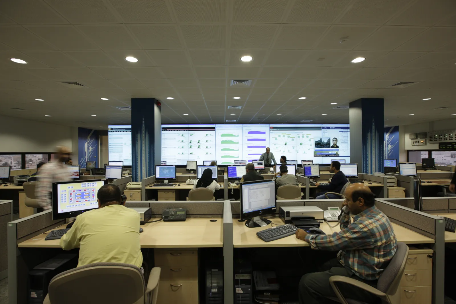
3. Collaboration across design centers without shipping data manually
A modern SoC is built by teams in multiple countries, often across an IP-supplier and foundry boundary. The old pattern - replicate the design database to each site, reconcile nightly, hope nobody is working against stale state - does not scale and is a correctness risk. A shared cloud data plane lets dozens of design centers work against one authoritative copy with consistent tooling (NXP / AWS).
The honest caveat: this only works if you also standardize. NXP stood up a cloud center of excellence for governance and standardization alongside the migration (NXP / AWS). Without a CCoE you get the worst of both worlds - shared infrastructure, inconsistent tool versions, and reproducibility problems at tape-out.
4. Protecting IP with confidential computing, not vague assurances
This is the section that usually gets hand-waved with "providers invest heavily in security." That is not an answer your security team will accept for GDSII or OpenAccess databases. The concrete, current mechanism is confidential computing: sensitive computations are isolated inside hardware-based Trusted Execution Environments via Intel SGX, AMD SEV, and AWS Nitro Enclaves, so data is protected not just at rest and in transit but in use (Confidential Computing: A Key To Secure Cloud And Edge Environments).
For semiconductor IP this is the control that makes the rest defensible: encrypted, access-controlled handling of the most sensitive design assets, mapped to the frameworks that actually bind your business - ITAR for export-controlled designs and GDPR where personal data is in scope. Design the residency and attestation requirements first, then choose the region and enclave technology that satisfy them. Treat any provider claim you cannot attest cryptographically as a claim you have to verify another way.
5. Pay-per-use economics that match a cyclical industry
Semiconductor demand is cyclical and project-driven. A fixed on-premises farm forces you to capitalize for the peak and amortize it across the trough. The cloud's pay-as-you-go model converts that capital expense into usage that tracks active projects - elastic scaling and on-demand provisioning replacing fixed capacity, which was an explicit driver in NXP's move off its own data centers (NXP / AWS).
Be precise about where the savings come from, because naive lift-and-shift can cost more than the on-prem farm it replaces. The wins are real when you (a) scale to zero between runs, (b) right-size instance families to each EDA step, and (c) keep tool-license utilization high so you are not paying for idle licenses while you pay for elastic cores. The economics follow the engineering discipline, not the migration itself. With AI network-fabric spending growing at a 38% CAGR from 2024 to 2029 (Deloitte), compute prices and instance options will keep shifting under you - another reason to keep capacity decisions reversible.
The bottom line
Cloud computing benefits the semiconductor industry not because it is fashionable but because the workload shape - bursty EDA, petabyte design state, globally distributed teams, export-controlled IP, and cyclical demand - maps cleanly onto elastic compute, parallel filesystems, a shared data plane, confidential computing, and consumption pricing. The proof points are in production at companies tapping out leading-edge silicon today, not in pilots. The teams that win the transition treat it as an engineering program - a cloud center of excellence, deliberate data placement, attestable security, and ruthless cost discipline - rather than a procurement decision.
If you are weighing a cloud migration for design, verification, or build infrastructure and want a clear-eyed assessment of the trade-offs, contact us to discuss how Expeditious Software can help.
Sources
- 2026 Global Semiconductor Industry Outlook - Deloitte Insights
- NXP Semiconductors Selects AWS to Drive the Next Era of Semiconductor Innovation - AWS / Amazon Press Center
- NXP Semiconductors Selects AWS as Its Preferred Cloud Provider to Power Electronic Design Automation in the Cloud - Business Wire
- Cloud EDA Market Size, Share and Trends 2025 to 2034 - Precedence Research
- Confidential Computing: A Key To Secure Cloud And Edge Environments - Semiconductor Engineering